No more secrets Part 2: Let us build the experimental board
Ingredients
- #1 Standard Breadboard (63 rows, 5+5 holes for row, power and ground rails
on both sides)
- #25 BC547 transistors
- #24 10Kohm 1/4W resistors (colors: brown=1 black=0 orange=10^3 gold=5%)
- #14 330ohm 1/4W resistors (colors: orange=3 orange=3 brown=10^1 gold=5%)
- #4 led diodes (Red, 5mm are okay)
- #2 electrolyctic capacitors 10uF (microfarad) 16V
- #1 5V power supply (the tool uses at most 250mA) (instead of a power supply you may consider using a battery holder for three or four AA batteries, everything should work at 4.5 or 6V).
- #1 set of jumpers for breadboards.
- #23 0.3" jumpers
A piece of old multi pair telephone wire can be used to create the jumpers, both the 0.3" wide and the longer ones to build the experiments.
Tools needed: cable cutter or a pair of strong scissors. If you have a wire stripper it is useful, although not strictly needed.
If you like, it is clearer during the experiments to provide the inputs using buttons instead of moving jumpers. In order to build a keypad for the input you need:
- #1 another breadboard (maybe smaller than the one above, I'm using a 30
rows one)
- #5 or more buttons for breadboards
- #5 jumpers (which can be created using the old telephone cable).
The board(s) implements:
- #1 1Hz master clock
- #11 NAND gates
- ... and #5 buttons on the second board
How to build the master clock
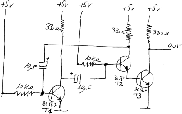
Schematics of the unit (already discussed in No_more_secrets_in_your_CPU:_Part_1|Part1):
For this unit you will need:
- #3 transistors
- #3 330ohm resistors (orange-orange-brown)
- #2 10Kohm resistors (brown-black-orange)
- #2 10uF capacitors
- #4 0.3" jumpers
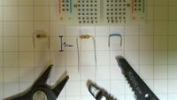
Fold the pins of the resistors and trim their length 10 about 1cm as illustrated below:
Resistors are not polarized (provided that the pins are connected in the right positions of the breadboard, you don't need to pay attention on which end is which).
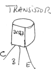
BC547 transistors are not cylindrical, they are flat on one side (usually there is the sign BC547 on that flat side). In order to recognize the three pins of a transitor (collector, base and emitter) you have to keep the transistor having the flat face towards you: in this position the three pins are C,B,E collector, base and emitter. (This is specific for BC547, other transistors may have different pin assignment).
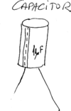
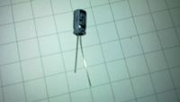
Electrolytic Capacitors are polarized. The negative lead is normally marked by a white stripe having multiple minus signs on it ("- - - ").
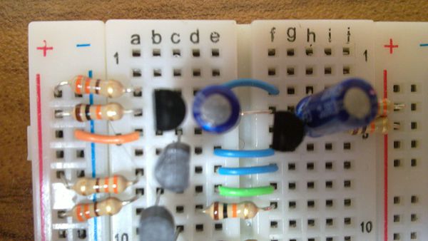
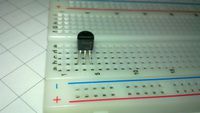
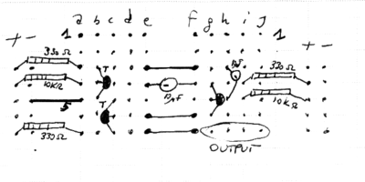
This figure shows how to insert the components on the breadboard.
Install all the components and jumpers on the Breadboard as shown in this picture:
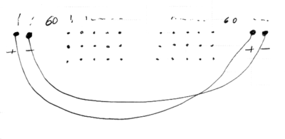
When all the components and the jumpers have been put on the breadboard, the circuit can be tested. Plug the power supply to the + and - rails on both sides (you can add jumpers to connect + and - of one side to the correspondent rails on the other). The blue rail should be connected to the negative, the red one to the positive.
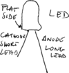
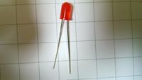
Now plug a led diode to the master clock's output: push the longest pin of the diode (its anode) in a hole of the output row and its shortest pin (the cathode) to a hole of the minus rail. Does it blink? I hope so. If it does your master clock is working, if it not blinking double check the position of all the components and jumpers.
How to build the 11 NAND gates
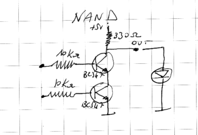
Schematics of the unit (already discussed in No_more_secrets_in_your_CPU:_Part_1|Part1):
For each gate you'll use:
- #2 transistors
- #2 10Kohm resistors
- #1 330ohm resistor
- #2 0.3" jumpers
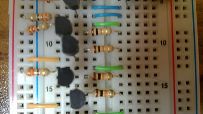
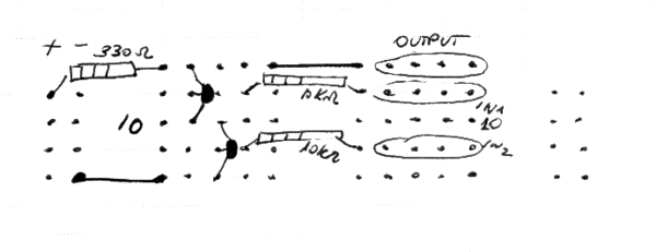
Insert the components as depicted (row numbers refer to the first NAND gate). Trim the pins of resistors before mounting them and pay attention to install trasistors in the correct direction.
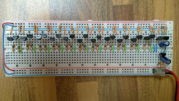
The same pattern should be repeated for all the other NAND gates. The first row of each gate is 8,13,18,23,28,33,38,43,48,53,58. For some gates the hole of the positive rail for the 330 ohm resistor or the hole of the negative row for the jumper are not aligned. Choose the closest available hole of the rail.
The following table maps each gate to the row numbers of its inputs and output.
 Gate In1 In2 Out
 CLK  --  --   7
 A     9  11   8
 B    14  16  13
 C    19  21  18
 D    24  26  23
 E    29  31  28
 F    34  36  33
 G    39  41  38
 H    44  46  43
 I    49  51  48
 J    54  56  53
 K    59  61  58
The circuit is complete. For the experiments we'll name the NAND gates using the letters of the alphabeth, A to K. The experiments will be carried out by adding jumpers to interconnect the gates and the master clock in a specific topology. All the inputs and outputs of the gates are connected to rows of the right-hand side of the breadborad, so it is possible to set up the experimental circuits by connecting the right rows on this side.
No other transistors, resistors, capacitors need to be further installed or existing components moved in order to build one by one the components of a CPU.
It is time to test the gates. Please test all of them because an error, a misfunctioning component or a false contact may prevent complex circuits from working properly.
For each gate: plug a led diode between the gate's output (the longest pin, i.e. its anode) and a hole of a negative rail (here plug the shortest pin of the led, its cathode). The led should be on. Now use two jumpers to connect both inputs of the gate to the positive rail. The led should turn off when both jumpers are connected. Now you can move the led and the jumpers to test the next gate. Should all of them work properly? If yes, be brave of you. You can move to the next stage and start experimenting on how these 11 NAND gates can work as signal routers, do computations, memorize, count and much more.
How to build the keypad (optional)
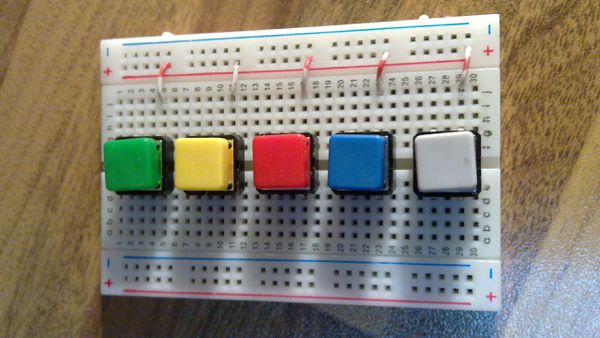
It is convenient to have a keypad to provide input to the circuits. Here is mine:
If you want to build one, take the second breadboard and connect one end of each the button to the positive rail.
Then connect the positive rail of the keypad to the positive rail of the main experimental breadboard.
The pin of each button which has not been connected to the positive rail can be used to provide an input bit to a circuit.
For example you can take the pin of two buttons and connect them to a NAND gate. When you push both buttons, a led installed on the NAND gate's output turns off.
A short note for real Electronic Engineers
I am a computer scientist, not an electronic engineer and this is an educational tool. I know that the design of real TTL and CMOS gates is quite different, from an electronic, not logical, point of view. The goal of this tool is to create a simple educational playground based on cheap and off-the-shelf components. BC547 are very common (at least in Europe (*)), while multiemitter transistors for TTL or typeN and typeP MOSFET for CMOS are less common.
Each gate of the experimental board always drains about 13mA to work. The current raises to 15mA when the output is zero. I am perfectly aware that these are huge values for the current to drive each gate but in this way it is possible to use a led diode as a logic probe.
(*) Many NPN transistors can be used instead of BC547. I have not tested it personally, but I am confident that 2N2222 should work. 2N2222 is a very common NPN transistor in the US.
