No more secrets Part E: Shift to Multiply and Divide
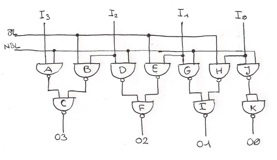
This is a left shift circuit for three bits:
and the jumper table:
in3 -> A
in2 -> BD
in1 -> EG
in0 -> JH
SL -> BEH
NSL -> ADGJ
A -> C
B -> C
C -> out3
D -> F
E -> F
F -> out2
G -> I
H -> I
I -> out1
J -> KK
K -> out0
To test this circuit exactly one of the inputs SL or NSL must be set to one. When NSL is one the 4 input bits are copied to the outputs. When SL is one in0 is copied to out1, in1 to out2, in2 to out3 and out0 is zero. If we give to the four input bits the meaning of the binary representation of a number, when SL is one the result is the input times two. The result is correct both for signed and unsigned numbers provided the result can be stored in four bits.
For esample:
leftshift(3) = leftshift(0011) = 0110 = 6 (both for unsigned and signed numbers)

leftshift(5) = leftshift(0101) = 1010 = 10 (unsigned only!)

leftshift(-3) = leftshift(1101) = 1010 = -6 (signed)
It is possible to test the circuit in this way: plug four leds on the output and connect NSL to one (positive rail). Now set a random input configuration, you'll see the same configuration in the pattern of leds. Moving the jumper from NSL to SL the led pattern will move (left) and the least significant bit will be zero.
A right shift circuit can divide values by two in a similar manner. Unfortunately, in this case signed and unsigned numbers must be processed in a different way.
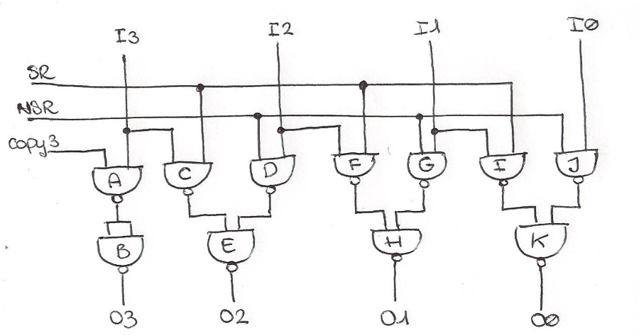
This is the circuit:
and the jumper table:
in3 -> AC
in2 -> DF
in1 -> GI
in0 -> J
SR -> CFI
NSR -> DGJ
copy3 -> A
A -> BB
B -> out3
C -> E
D -> E
E -> out2
F -> H
G -> H
H -> out1
I -> K
J -> K
K -> out0
Now the valid configurations for SR, NSR and copy3 are the following ones:
SR NSR copy3
0   1   1     copy all the inputs in the corrisponding outputs
1   0   0     shift right for unsigned (the MSB is zero)
              (also known as logical shift)
1   0   1     shift right for signed (the MSB is copied)
              (A.K.A. arithmetic shift)
The difference between a logical shift and an arithmetic shift is the management of the Most Significant Bit (MSB, i.e. out3): a logical shift resets it to zero while an arithmetic shift copies the former value of the MSB, out2 and out3 has always the same value in an arithmetic shift. In other words, an arithmetic shift keeps the sign bit unchanged.
A logical right shift is a division by two operation for unsigned integers. An arithmentic right shift is a division by two only for positive integers and for even negative numbers. For odd negative numbers the result is rounded downwards, so incorrect.
(any kind of right shift, logical or arithmetic).
rightshift(3) = leftshift(0110) = 0011 = 3
(both for unsigned and signed numbers)

logical_rightshift(10) = logical_rightshift(1010) =
    = 101 = 5 (unsigned only!)

arithmetic_rightshift(-6) = arithmetic_rightshift(1010) =
    = 1101 = -3 (signed)

arithmetic_rightshift(-3) = arithmetic_rightshift(1101) =
    = 1110 = -2 (signed)
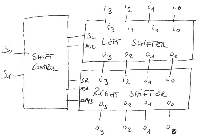
A complete and flexible shifter can be implemented using three breadboards.
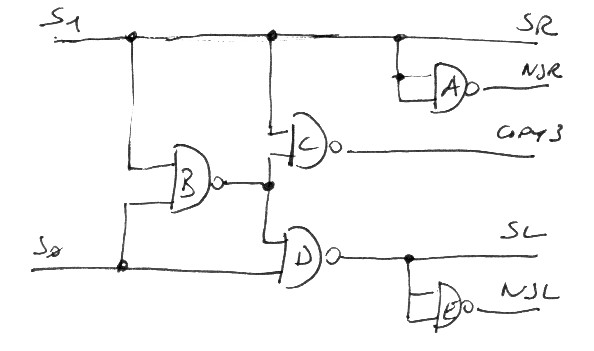
The shift control circuit has two control bits sh0 and sh1 supporting the following configurations:
sh1 sh0
0   0   do not shift
0   1   left shift
1   0   (logical) right shift
1   1   arithmetic right shift
This is the circuit and the map for the jumpers:
sh1 -> AABC outSR
sh0 -> BD
A -> outNSR
B -> CD
C -> outcopy3
D -> EE outNSL
E -> outSL


