No more secrets in your CPU: Part 1
This is the first of a set of postings. I am writing here, on my BLiki, the draft of a booklet about Computer Architecture in the spirit of "Making".
This booklet describes an educational tool created to reveal the secrets of the basic elements of digital computers.
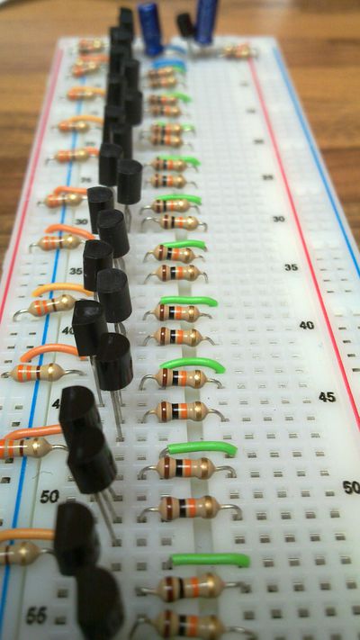
This is a picture of the "tool", just to whet your appetite.
Nothing magic happens in the processor of your computers, it is just a matter of circuits an commutation of electric currents. Everything works using an elementary switching device: the transistor.
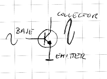
A transistor is an electronic component which is able to drive a high current on the basis of a low control current. It is basically an amplifier. The control pin is the base (B), the reference gate is the emitter(E), the output gate is the collector(C).
The low control current flowing between the base and the emitter, enables a high current between the collector and the emitter. For NPN transistors, the ones we use, these currents are positive (the potential, or voltage of the Base and Collector is higher than the potential of the Emitter). The symbol of a NPN transistor has the arrow of the emitter pointing outwards. There are other transistors named PNP, having the inwards arrow in their symbol. PNP transistors use negative currents instead of positive currents.
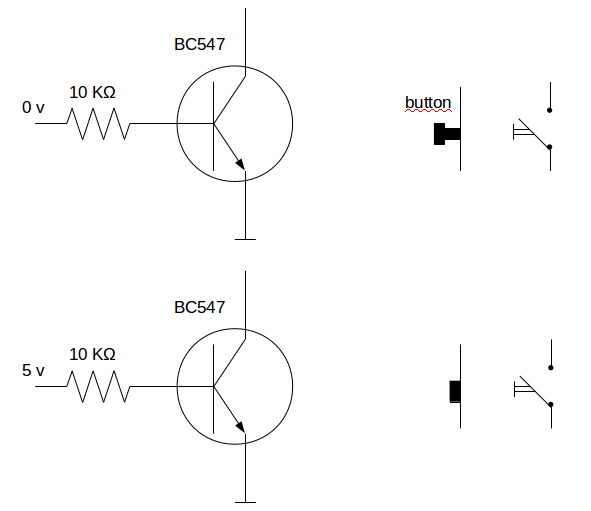
For our purposes we will use our transistors as binary switches. In fact a current of 0.5mA (almost) saturate a transistor of the type used in our experiemental tool (BC547). A transistor behaves like a remotely controlled finger pushing a button. When a current flows through the transistor's base the finger pushes the button, otherwise it keeps it released.
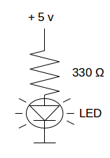
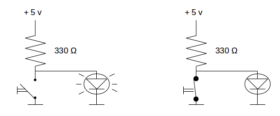
Let us consider this circuit:
The current flows through the resistor and the led diode which turns on. The resistor in this circuit limits the current so that the diode cannot be damaged.
Let us add a button to the previous circuit in this way:
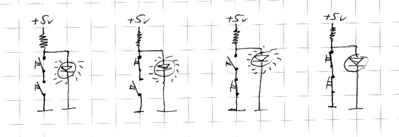
If you push the button, the current flows through the button where the resistence is null instead of passing through the diode. As a consequence, the led turns off. If we use two buttons connected as depicted here below (in series), the led diode turns off when both buttons get pushed.
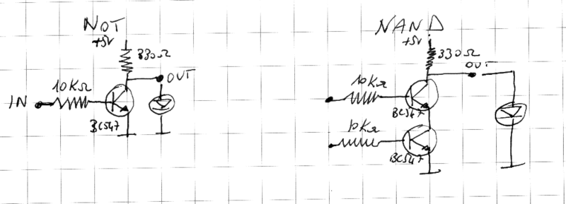
We have said that a transistor may work as a remotely controlled finger which pushes a button, so we can redesign the circuits about using transistors in lieu of buttons.
As we will see almost all the components of a CPU (a processor) can be built using a large number of these circuits. More precisely the circuit using two transistors is a basic brick that can can be used to build all the others.
The circuit on the left, having one input and one transistor, is a NOT gate. It negates its input: when its input is connected to the positive pin of the power supply (+ 5V) the output is 0V. If there is a led connected it is off. Viceversa if the input is connected to the negative pin (0V), or left not connected, the output is 5V, the led is on. We will call 0V as the logical state 0 and the logical state 1 is +5V.
The logical table of a NOT gate is:
 IN OUT
 0  1
 1  0
The second circuit is a Not AND, usually abbreviated as NAND. Its logical table is:
 IN1 IN2 OUT
 0   0   1
 0   1   1
 1   0   1
 1   1   0
In fact, in plain English the semantics of the conjunction "and" is that a sentence consisting of two statements connected by an "and" is true if both statements are true, it is false otherwise. Our logic gate returns exactly the opposite result of an "and", if returns 1 when an "and" returns 0 and viceversa. It is a Not AND, the negation of an AND. Almost all (say all but one) circuits of a modern computer can be built using NANDS.
For example, if the two inputs of a NAND gate are connected together the circuit has the effect of a NOT. In this case, in fact, either both inputs have value 1 or both value 0. Our "remotely controlled fingers" are tied together so either both buttons are pushed or none. So, it is not necessary to have a specific circuit for a NOT.
However, one relevant circuit cannot be built using NANDs: the master clock. A computer includes a lot of components able to perfom computations, activate/deactivate functions. route data, store data etc. but all these elements need a director. Like an orchestra, a processor requires a component which provides all the instruments/elements with a rhythm, a pace so that the result can be either a synphony or a computation and not a chaos. Every element has to perform its task in a synchronized manner. Our director, however, has not a complex score to follow, it simply generates a square wave, a coninuous sequence of 0 and 1 one following the other always at the same pace or frequency. When the advertisement of a computer says that it runs at one two or three GHz (giga herts) it means that its director's stick goes up and down one, two or three billion times per second.
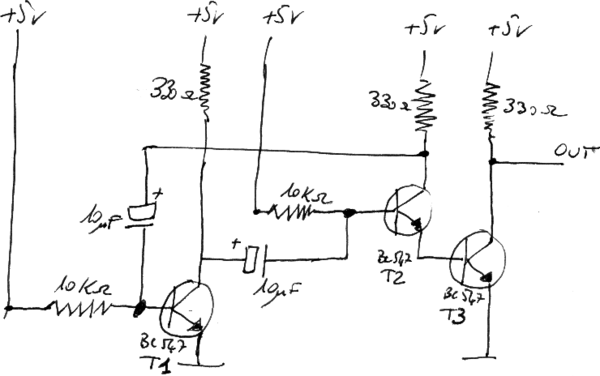
This is the circuit of our master clock:
The circuit has been drawn to show the similitudes with our previous circuits. If we forget for a moment the two capacitors, the circuit configuration of the first transistor on the left (T1) is a NOT circuit. It has its input forced to the value 1, then its output without the capacitors would be 0. Still watching the circuit without the capacitors, the other part of the circuit would behave in a similar manner. The base of the transistor in the middle (T2) is connected to 1 so a current can flow through its emitter and then throw the base-emitter junction of the transistor of the right (T3). As a consequence, both transistors "close" their circuits, thus the output and the collector of the transistor in the middle are at logical level zero.
The capacitors work as small batteries. When the output at the collector of T1 transistor is 0v, the capacitor at the base of T2 is charging. Thic capacitor requires a lot of current to start charging and then the current decreases as its tends to complete its charge. As a consequence at the beginning of the charge process the potential at the base of the transistor is close to zero and then it slowly reaches 5 volts. When the potential at the base of T2 is 0, T2 and T3 are open, but after a while, when the current reaches a certain level, they switch. When T2 and T3 close, the potential at the collector of T2 drops to zero volts causing the other capacitor to start charging. The current needed to charge this capacitor force the potential at the base of T1 to 0v. T1 opens the circuit. The output at the collector of T1 goes to one, i.e. 5v. The other capacitor is discharging. After a while, when the capacitor on the left reaches a certain level of charge T1 flips and closes its circuit. The output at its collector returns to 0v and the cycle can be repeated from the beginning.
So, why we need T3? The output at the collector of T2 would be very different from a square wave. In fact, due to the current flowing through the capacitor the rising edge of the wave would be very slow. When T2 has just begun to switch, at the beginning of the rising edge, the current is enough to force T3 to switch completely. When our remotely controlled finger is still lightly touching T2, T2's finger gives a strong push to T3.
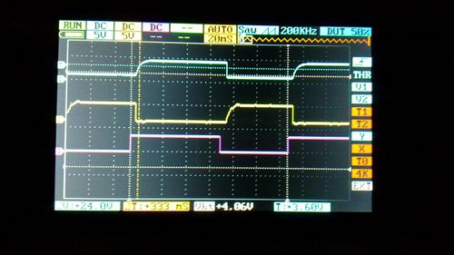
This is a snapshot of my portable oscilloscope.
The top trace (blue) is taken at the collector of T2, the second trace (yellow) is taken at the collector of T1 while the third (pink) is the trace of a logical analyzer connected to the output (collector of T3). As you can see the rising edge are quite smooth in the blue and pink traces, not square waves at all. These two traces show how T1 and T2 continue to swing between their two states open/close. T3 makes the rising edge steeper. It is not a perfect square wave, but nothing is perfect in electronics.
The values of the components have been chosen to have a clock beating at a frequency around 1Hz, i.e. 1 cycle per second. It is much slower than the clocks of our personal computers, tablets or portable phones, but the idea is the same. The purpose of this educational tool is to show how all the basic components of a CPU work. Phenomena changing at the rate of 1Hz or less can be easily observated by humans. Our master clock frequency in not exactly 1Hz and can slightly change during the time. In fact, the values of the components are subject to a tolerance and can vary due to the temperature. Real master clocks use the electrical obscillations of a quartz crystal to provide a square wave at a quite stable frequency.
