No more secrets Part 10: Synchronous memory
The computational circuits generate a binary output depending (only) on the value of their inputs. These circuits are called combinatorial circuit because their output does not depend on the time. Providing them with a specific input data configuration, they give the same result. Oue ALU is an example of combinatorial circuit: for a given configuration ot its input pins (data and control pins) it always generates the sale output.
A closer look of a combinatorial circuit would reveal that it need a bit of time to converge to its result, the time neede by all the logical gates to switch to their new status.
A memory to store the current status is the trick to generate sequential circuits. The current status is used by the combinatorial circuits to compute the next status which is stored in the memory for the next step.
In order for this circuit to work properly, the status storage circuit must be composed by cells able to store the new status and to give the old status at the same time, otherwise the output of the current computation could be erroneously taken immediately as input of the computation itself. So if the combinatorial circuit, for example, adds one to the former status, the new value could be taken erroneously as input and add two, three, etc. resulting in a unpredictable result. It would play like an orchestra without a director.
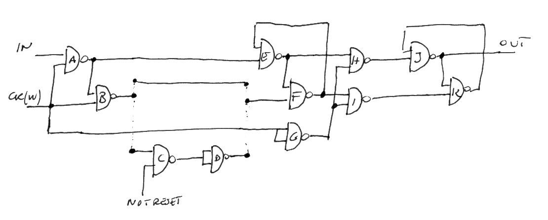
This is the goal of the master-slave flip-flop (MSFF). Here is the schematics of a MSFF. (The reset part is optional. It will be described below.)
in -> A
w(ck) -> ABGG
(notreset -> C)
A -> BE
B -> F (or B -> C)
(C -> DD)
(D -> F)
E -> FH
F -> EI
G -> HI
H -> J
I -> K
J -> K out
K -> J
This circuit is composed by two latches. The first (composed by gates E and F) is storing the new value when ck is one, the second (gates J and K) copies the value of the first latch when ck drops to zero.
In this way, when ck is one the combinatorial circuit can compute a new value which is stored in the first latch. In fact, when ck is one the two latches are insulated and can have different values stored. So, status changes made by the combinatorial circuit are stored in the first latch but cannot be propagated again in the combinatorial circuit as inputs. In other words, the input of the combinatorial circuit is stable.
When ck switches to zero the value of the first latch becomes stable and is copied in the second latch. When ck is zero, the input in of the MSFF is ignored.
The optional circuit composed by gates C and D adds an input pin to reset the flip-flop. Our MSFF workd properly when the pin notreset is one, i.e. it is connected to the positive rail of the breadboard.
If notreset is temporarily set to zero our MSFF value is reset to zero. This pin can be used to force the MSFF to have value zero when the circuit is powered up. Without this circuit, a flip-flop, and in general any latch, has an initial random value, zero or one, depending on which gate of the latch converges first. Many circuts can have random initial values, but some do not. It is the case, for example, of the program counter, the register which stores the address of the next instruction to be executed. A register in our CPU is an array of MSFF. This register must have a pre-determined value at startup; zero can be a good choice.
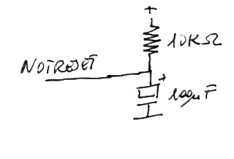
If we connect the notreset pin to a circuit like the following one:
our flip-flop will always have out equals to one when the circuit is turned on. In fact, at startup notreset will be zero until the capacitor has been charged to the one level and then it will be one forever.
To test our MSFF connect the notreset pin to one (or to the circuit above if you have implemented it). Then connect two leds at the outputs of gates E and J and buttons conencted to in and ck(w). Now, decide which value you want to store in our FF. If it is one push the button connected to in, otherwise leave it unpushed. Now, keeping the in button in that state, push the ck(w) button and keep it pressed for a while to better understand how this circuit works. You should see the value connected to the E gate chenging its state to assume the same value as in. The led connected to the E gate showd the status of the first latch, it has been added just for educational purposes, it is not a real output of the system. The value of out is shown by the led connected to the J gate, this value does not change while ck(w) is one.
When the button connected to ck(w) is released, the value of the first latch is copied to the second, so the output led (connected to gate J) gets the same status of the other led.
You can also connect the ck(w) the master clock and a third led to the output of the clock. You will see that the input provided by the in button is copied in the master latch (gates EF) when the clock is one and then to the slave latch (JK) when the clock shitches to zero.

