No more secrets Part 3: A NAND is for everything
In the first experiment we'll use our 11 nand gates to implement all the types of gates.
The following table includes for each gate type:
- its name
- its symbol for logic and electronic schematics
- the schematics of a circuit using only NAND ports which implements that
gate.
- the truth table
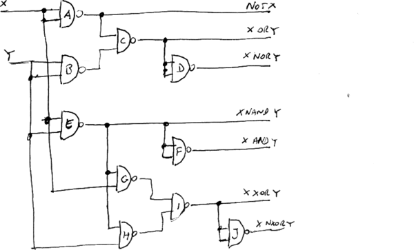
The following circuit can be implemented on the breadboard and implements all the logic gate of the previous table.
We'll use this test circuit to explain the notation used to describe which jumpers must connect on the breadboard to set up the experiment.
The table include a row for each input signal and one row for each gate used.
X->AAEG
means that the input X must be connected to both inputs of the A gate, and to one input of E and G
E->FFGH out5
means that the output of gate E must be connected to both inputs ot the F gate and to one input of gates G and H. The output of gate E is also an output line of the circuit.
The complete table for this circuit is:
 X->AAEG
 Y->BBEH
 A->C out1
 B->C
 C->DD out2
 D->out3
 E->FFGH out4
 F->out5
 G->I
 H->I
 I->JJ out6
 J->out7
As a rule of thumb, a basic consistency test on this table consists in checking that each gate appears exactly twice on the right side of the arrows. In fact the output of a gate can be connected to several inputs ot other gates. Gate outputs should never be connected together.
 out1 is NOT(X)
 out2 is X OR Y
 out3 is X NOR Y
 out4 is X NAND Y
 out5 is X AND Y
 out6 is X XOR Y
 out7 is X NXOR Y
Now it is possible to put a led on one of the output lines, and test all the possible configurations for X and Y, (0,0), (0,1), (1,0) and (1,1).
The led should turn on and off consistently with the truth table for that specific gate.


